In this chapter, we will explain the basic building blocks of a simple computer system. In the subsequent chapters, we will construct progressively more complicated CPU’s out of these components.
2.1 Registers
An n-bit register is a hardware data storage unit which can store an n-bit number. If we have an n-bit data in our hand and want to preserve it for future use, we can store it into an n-bit register. The register will remember that data until some other data is written into it, in which case it will be erased and lost.
The simplest n-bit register has three input ports: DATAIN (n bits wide), CLOCK (1 bit wide), and LOAD (1 bit wide). It has a single output port: DATAOUT (n bits wide). The schematic for a 4-bit register is given below:
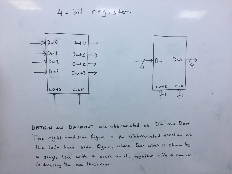
The register pictured above will store 4-bits of data, and that 4-bit data can be seen at its DATAOUT port. As long as LOAD is 0, the register will continue to keep this data. The data at the DATAIN port will not have any effect.
If we want to write new data to the register, we place this new data into the DATAIN port, make LOAD=1, and wait for the arrival of the next CLOCK edge. At the next clock edge, the data in the DATAIN port will be written into the register and will immediately appear in the DATAOUT port. The previous data will be lost.
If LOAD=0, no data will be written into the register. The register will keep on remembering the data it already contains.
2.1.1 How to construct a register
Registers are constructed from flip-flops. It is possible to construct registers by using any type of FF’s: T, D, JK, SR, etc will all do. We will use SR FF’s, as this is the simplest case.
Below is a 1-bit register constructed via SR-FF’s:Its operation is as follows:
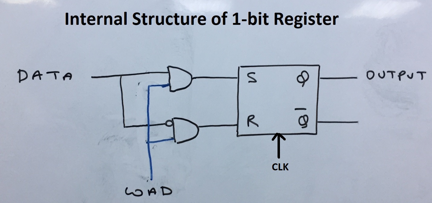
- When LOAD=0, SET and RESET inputs of the SR-FF are both zero, irrespective of the DATA input. Hence the SR-FF will not change its contents in the next clock edge. It will continue to remember its present contents.
- When LOAD=1 and DATA=0, SET will become zero and RESET will become one. In the next clock edge, the FF will reset.
- When LOAD=1 and DATA=1, SET will become one and RESET will become zero. In the next clock edge, the FF will set.
We can summarize this as follows: When LOAD=0, the 1-bit register will continue to remember its current contents. When LOAD=1, it will forget its current contents and will take in the data waiting at its DATA input.
Note that in this circuit the SR_FF will never receive the forbidden input SET=1, RESET=1.
An n-bit register is formed by connecting n 1-bit registers in parallel. A 16-bit register drawn in Logisim is given below as an example.

2.1.2 Registers with increment
A more complicated type of register is “the register with increment”. In addition to the normal ports of a register (DATAIN, DATAOUT, LOAD, CLOCK) it has an additional 1-bit INCREMENT input. Its schematic is given below:
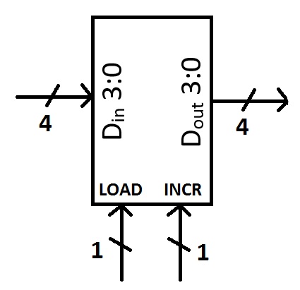
Its operation is as follows
- If LOAD=0 and INCREMENT=0, it will continue to preserve the data it contains and will disregard its DATAIN port.
- If LOAD=1 and INCREMENT=0, it will load the data in its DATAIN port at the arrival of the clock edge. The previous data it contained is lost.
- If LOAD=0 and INCREMENT=1, it will increment the data it contained at the arrival of the clock edge. The DATAIN port is ignored.
- LOAD=1 and INCREMENT=1 is illegal and should never be used.
2.1.3 How to construct a register with increment
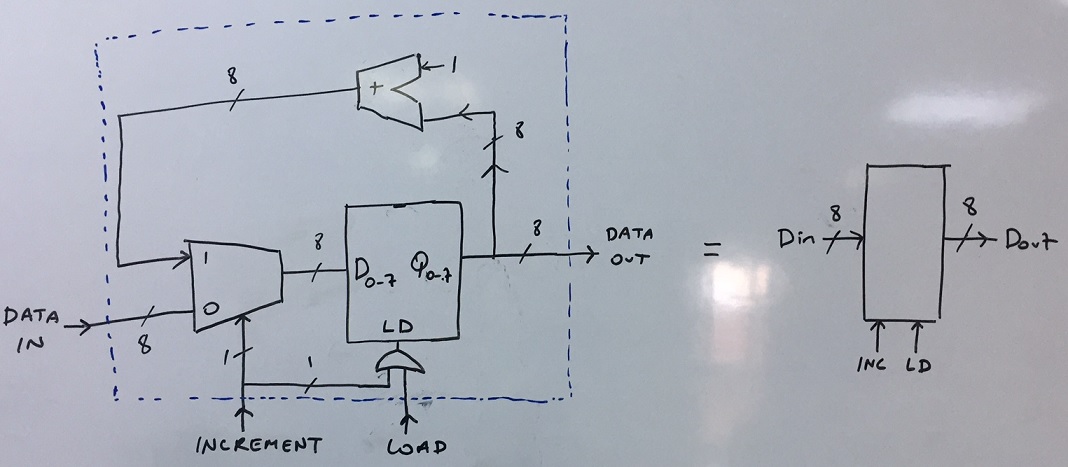
A register with increment can be constructed from a normal register by the addition of an adder, a multiplexer and an OR gate. The construction for an 8-bit register is shown below.
2.1.4 Register with increment and decrement
This kind of register is obtained by the addition of a DECREMENT input to the register with increment.
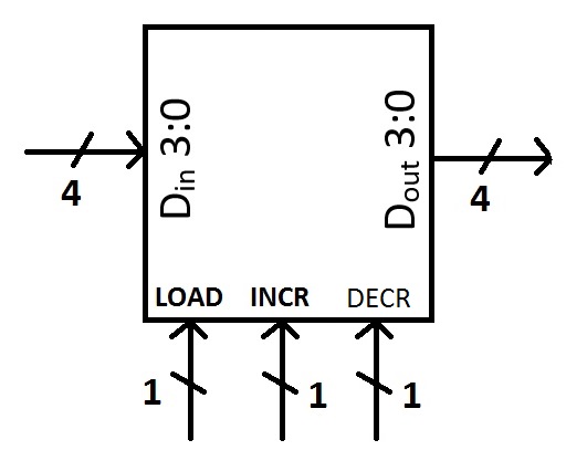
Its operation is obvious and will not be explained here. Note only that only one of the LOAD, INCREMENT and DECREMENT inputs can be 1 at any given time. If all of them is zero, the register will continue to keep its contents.
Homework: Construct a 4-bit register which can increment and decrement.
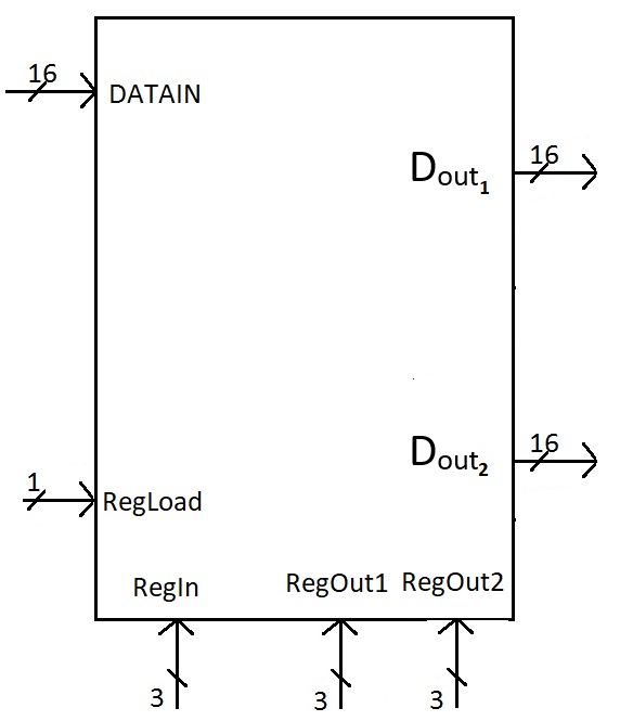
2.2 Register Banks
A register Bank (also called a Register File) is a hardware circuit which consists of many registers. It is possible to write into any of these registers at a given clock edge. It is possible to read all of these registers at all times.
A register bank with n k-bit registers has n+3 ports:
- REGWRITE: If any one of the registers is to be written in the next clock edge, this signal becomes 1. Otherwise, it is kept at 0.
- REGSELECT: Selects which register is to be written. The number of the register to be written is to be entered here. If we have k registers, this signal is log2k bits. Example: If we have 32 registers in our register bank, this signal is 5 bits. If we want to write to register 13 then REGSELECT=01101, Takes effect only when REGWRITE=1.
- DATAIN: k-bit input port. The data that is to be written into a register of the register bank must be put here.
- DATAOUT[n]: The contents of register j is continuously displayed at DATAOUT[ j ], which has k bits.
Note that only one register can be written at a given clock edge, as there is only one data input port. But the data contained in all registers can be seen simultaneously, as all the registers have their own data output ports.
The schematic of a register bank is shown below:
To summarize, the basic operation is as follows:
- If we want to read register j in the register bank, we just read the port DATAOUT[ j ]. Read operation is independent of the clock.
- If we want to write new data into register j, we put the data into the DATAIN port, we put the register number j into the REGSELECT port, and we make REGLOAD=1, and wait for the clock edge. After the clock edge, the data will be written into register j and that data will be displayed at port DATAOUT[ j ].
Example: The register bank below has 16 registers, and each register has 16 bits. We want to write 0x21A4 into register 14. Then we make DATAIN=0x21A4, REGSELECT=0xE, REGLOAD=1 and wait for the next clock edge. After the clock edge, the data will be written into register 14 and will be displayed immediately at DATAOUT[14].
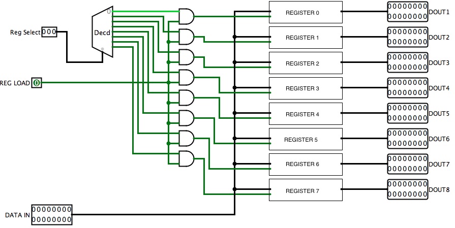
2.2.1 Internal structure of register banks
2.2.2 Register bank with special registers.
There are two more features which we may want to add to register banks:


-
We may want to increment and decrement some given registers in the register bank.
-
We may want to set end reset some bits in some given registers of the register bank.
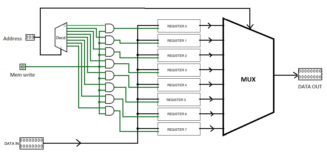
2.3 Memory
Memory acts like a huge register bank. The only difference with the register bank described above is that there is a multiplexer at its output.

The internal construction is
2.4 Arithmetic Logic Unit (ALU)
In chapter 1, we have investigated nine different hardware circuits which are capable of performing various Arithmetic-logic operations . These circuits are
- Adder (+)
- Subtractor (-)
- Bitwise And (&)
- Bitwise Or ( |)
- Bitwise Xor ( ^ )
- Bitwise Not (!)
- Move ( <- )
- Inc (++)
- Decrement ( — )
Arithmetic-logic unit (ALU) is a super-circuit which is capable of performing all the above AL operations.

| ALU Operation Code (Binary) | ALU Operation | Explanations |
|---|---|---|
| 0000 | Res = Din1 + Din2 | Twos Complement 16 bit addition |
| 0001 | Res = Din1 – Din2 | Twos Complement 16 bit subtraction |
| 0010 | Res = Din1 & Din2 | 16 bit bitwise AND |
| 0011 | Res = Din1 (or) Din2 | 16 bit bitwise OR |
| 0100 | Res = Din1 ^ Din2 | 16 bit bitwise XOR |
| 0101 | Res = ! Din1 | 16 bit bitwise negation |
| 0110 | Res = Din1 | Data Movement |
| 0111 | Res = Din1 + 1 | 16 bit twos complement increment |
| 1000 | Res = Din1 – 1 | 16 bit twos complement decrement |

