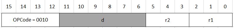
It is quite possible to increase the number of registers of reptile to 8 without compromising on any other specification. If you remember our previous lectures, the main limiting factor on the number of registers of reptile was the ALU instruction. There are three varieties of the ALU instruction:


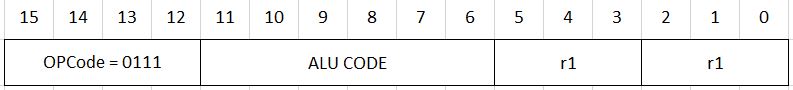
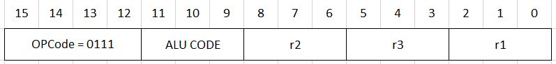
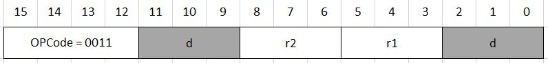
If the number of registers are increased from 4 to 8, r1, r2 and r3 fields will widen from 2 to 3 bits. While this will not create any problems for the first two formats, three-bit register fields will not fit into the third format.
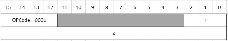
Machine Code Format for LDI
LDI r,x
Machine Code Format for INC and DEC
INC r1
Machine Code Format for MOV and NOT
MOV r1 r2
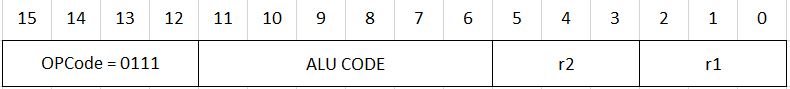
Machine Code Format for ADD, SUB, AND, OR, XOR
ADD r1 r2 r3
Machine Code Format for LD
LD r1 r2
Machine Code Format for ST
ST r1 r2
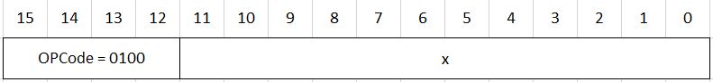
Machine Code Format for JMP
JMP x
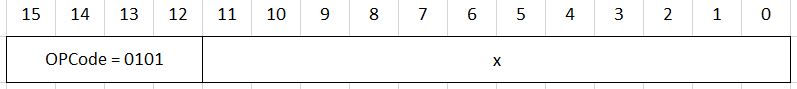
Machine Code Format for JZ
JZ x
Reptile Verilog Code
//Reptile design with 8 Registers.
// This module also sents register #0 to main module as an output
module reptile (
input clk,
input [15:0] data_in,
output [15:0] data_out,
output logic [11:0] address,
output memwt,
output [15:0] reg0
);
logic [11:0] pc, ir; //program counter, instruction register
logic [4:0] state; //FSM
logic [15:0] regbank [7:0];//registers
logic zeroflag; //zero flag register
logic [15:0] result; //output for result
localparam FETCH=4'b0000,
LDI=4'b0001,
LD=4'b0010,
ST=4'b0011,
JZ=4'b0100,
JMP=4'b0101,
ALU=4'b0111;
logic zeroresult; //zeroflag value
always_ff @(posedge clk)
case(state)
FETCH:
begin
if ( data_in[15:12]==JZ) // if instruction is jz
if (zeroflag) //and if last bit of 7th register is 0 then jump to jump instruction state
state <= JMP;
else
state <= FETCH; //stay here to catch next instruction
else
state <= data_in[15:12]; //read instruction opcode and jump the state of the instruction to be read
ir<=data_in[11:0]; //read instruction details into instruction register
pc<=pc+1; //increment program counter
end
LDI:
begin
regbank[ ir[2:0] ] <= data_in; //if inst is LDI get the destination register number from ir and move the data in it.
pc<=pc+1; //for next instruction (32 bit instruction)
state <= FETCH;
end
LD:
begin
regbank[ir[2:0]] <= data_in;
state <= FETCH;
end
ST:
begin
state <= FETCH;
end
JMP:
begin
pc <= pc+ir;
state <= FETCH;
end
ALU:
begin
regbank[ir[2:0]]<=result;
zeroflag<=zeroresult;
state <= FETCH;
end
endcase
always_comb
case (state)
LD: address=regbank[ir[5:3]][11:0];
ST: address=regbank[ir[5:3]][11:0];
default: address=pc;
endcase
assign memwt=(state==ST);
assign data_out = regbank[ir[8:6]];
always_comb
case (ir[11:9])
3'h0: result = regbank[ir[8:6]]+regbank[ir[5:3]]; //000
3'h1: result = regbank[ir[8:6]]-regbank[ir[5:3]]; //001
3'h2: result = regbank[ir[8:6]]®bank[ir[5:3]]; //010
3'h3: result = regbank[ir[8:6]]|regbank[ir[5:3]]; //011
3'h4: result = regbank[ir[8:6]]^regbank[ir[5:3]]; //100
3'h7: case (ir[8:6])
3'h0: result = !regbank[ir[5:3]];
3'h1: result = regbank[ir[5:3]];
3'h2: result = regbank[ir[5:3]]+1;
3'h3: result = regbank[ir[5:3]]-1;
default: result=16'h0000;
endcase
default: result=16'h0000;
endcase
assign zeroresult = ~|result;
assign reg0=regbank[0];
initial begin;
state=FETCH;
zeroflag=0;
pc=0;
end
endmoduleMain Module for Reptile
//This module sents Register #0 to seven segment display

module top_module (grounds, display, clk, pushbutton,led);

    input   pushbutton;
    output  [3:0] grounds;
    output  [6:0] display;
    input   clk;
    output led;

    //  memory chip
    logic     [15:0] memory [0:127];

    // cpu's input-output pins
    logic     [11:0] pc; //for debugging
    logic     [15:0] data_out;
    logic     [15:0] data_in;
    logic     [11:0] address;
    logic     memwt;

    logic     [15:0] reg0;

 assign led=memwt; //check memory write signal works or not. For debugging

    //instantiation of cpu
  reptile rr1 (.data_in(data_in), .data_out(data_out), .clk(~pushbutton), .memwt(memwt), .address(address),.reg0(reg0));
    //instantiation of seven segment
    sevensegment ss1 (.grounds(grounds), .display(display), .clk(clk),  .datain(reg0));


    assign data_in=memory[address];

	 always_ff @(posedge clk)
		if (memwt==1)
			memory[address]<=data_out;


    initial begin
		$readmemh("ram.dat", memory);
    end

endmodule